**This article is provided by Prof. Feng Jicheng, and is originally published on the Materials Community of Springer Nature on August 16
High-performance electronics requires billions of transistors, but their downsizing and interconnections, and materializations impose technological limits. Three-dimensional (3D) printing at nanoscale can probably provide a solution.
Convergence between 3D printing and nanotechnology
In today’s fast-evolving technological landscape, microscopic innovations catalyze monumental advancements. The study of 3D nanoarchitectures has been creating ripples across nanophotonics and nanoelectronics. These infinitesimally small constructs allow us to explore interactions between light and matter at scales never thought possible. However, traditional methods for making nanostructures face severe limitations in material choices, processing time, and structural flexibility, hindering progress in nanophotonics and nanoelectronics. The 3D nanoprinting technology proposed by Assistant Professor Feng Jicheng’s group in SPST, as reported in the article entitled “Metal 3D nanoprinting with coupled fields” in Nature Communications, introduces a fundamentally different approach, addressing these challenges and enabling efficient, high-precision, and scalable fabrication of diverse nanoarchitectures, redefining the paradigms of nanomanufacturing.
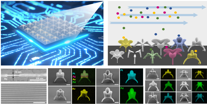
Powering next-generation of nanoelectronics and nanophotonics with the key abilities to print multiple materials of high precision. The scale bar is 1 μm, unless otherwise specified.
Feng’s group, Aerosol Intelligence Laboratory (AIL), aims at mapping out the future of system-level integration with new nanoprinting solutions. Their 3D nanoprinting technology, which was coined as Faraday 3D printing, opens up the vast potential of multi-materials printing, which was largely elusive until now. Adjusting electric and flow fields provides a high degree of flexibility in materials—from single metals to alloys and multi-materials. The technology can now tailor the optical properties of the printed nanoarchitectures by adjusting the material, geometry, feature size, and array periodicity.
Key innovations
The groundbreaking 3D nanoprinter uses of a double-layer flow whereby one layer carries the aerosol while the other layer, which is adjacent to the substrate, flushes neutral aerosol particles away from the substrate surface while charged ones follow the field lines and be deposited to precise locations. This design not only makes an end product unobscured by the random attachment of neutral particles to either the substrate or emerging structures, but also exerts the capability for size-selection of the charged aerosol particles. Such size-selection eliminates the material influence, as the motion of charged particles with given sizes is independent of materials. This in situ printing overcomes material restrictions, limited downsizing capability, and low efficiency encountered in traditional nanomanufacturing techniques. The new methodology favors to work in the dry-gas environment, thus preserving material purity, eliminating the need for complex post-treatment. Notably, the 3D nanoprinter powerfully enables the possibility to fabricate 8000 × 8000 uniform 3D nanostructures within a brief time frame of 20 minutes and boasts of the finest linewidth ever reported—an astounding 14 nm.
The diversity of materials it can handle is stunning—Au, Ag, Pd, Pt in the single type category and Au–Ag, Ni–Ti, Ni–Cr–Co–Mo–Ag in the alloy type. Complex nanoarchitectures previously constrained by cost and complexity can be now fabricated efficiently. With its ability to print uniform 3D nanostructures at an industrial scale, this high-speed, cost-effective printer offers a realistic alternative to extreme ultraviolet (EUV) lithography, a dominating powerhouse in improving computational power and energy efficiency.
The advent of this self-developed 3D nanoprinter is more than a scientific innovation—it is a revolution that upends current norms and sets the stage for a wave of advancements in nanotechnology and atomic-level manufacturing. By integrating the printer into semiconductor assembly lines, engineers can accelerate the one-pass printing of micro-bumps and interconnects with nanometer feature sizes on a wafer scale.
The coming future: Embracing 3D nanoprinting and global synergies
It is believed that transitioning from lithography to 3D printing in the realm of nanoelectronics and nanophotonics represents a paradigm shift, defining the central research challenges of the future. To address these challenges, it is imperative to concentrate on fundamental advancements in materials, devices, processing, and the design and fabrication of highly complex systems.
The fascinating realm of modern 3D printing has evolved, and the ability to work with multi-materials at nanoscale precision is now a reality. As Feng’s group venture deeper into the intricacies of nanophotonics/plasmonics and nanoelectronics, the potential for transformative developments is immense.
This study is completed with the collaboration of Dr. Vasanthan Devaraj from Pusan National University. Liu Bingyan, a first-year Ph.D. student in SPST, is the first author of the paper, and Prof. Feng Jicheng is the corresponding author.